
CAE Software【Femtet】Murata Software Co., Ltd.
Example10 Multi-Step Thermal Load Analysis for IC Soldering Process
General
-
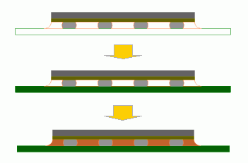
An IC is underfilled after mounted and soldered on a substrate.
The process involves several temperature changes. The mechanical stresses during the process are analyzed. -
The reached temperature is set on each step. Bodies can be included in the analysis at a specific step.
-
Using the same model, mechanical stress analysis with solder’s elasto-plasticity and creep taken into account is explained in
Exercise 8: Mechanical Stress Analysis of Operating IC after Soldering
-
The distributions of the displacement and the mechanical stress are solved for each temperature.
-
Unless specified in the list below, the default conditions will be applied.
Analysis Space
|
Item |
Settings |
|
Analysis Space |
2D |
|
Model unit |
mm |
Analysis Conditions
To simplify the analysis, the 2-D model is analyzed.
Select the thermal load option.
|
Item |
Settings |
|
Solver |
Mechanical Stress Analysis [Galileo] |
|
Analysis Type |
Static analysis |
|
Options |
Select “Thermal load”. |
The process is as follows.
Step 1 The IC is soldered on the substrate at 220[deg] and cooled down to 25[deg].
Step 2 The temperature is increased from 25[deg] to 120[deg].
Step 3 At 120[deg], the underfill is applied and hardened. After the hardening, the temperature is decreased to 25[deg].
Step 4 The temperature is increased from 25[deg] to 85[deg].
The Step/Thermal Load tab is set as follows.
The temperature profile is set as follows.
|
Tabs |
Setting Item |
Settings |
||||||||||||||
|
Step/Thermal Load |
Step Setting |
Multi-step thermal load analysis |
||||||||||||||
|
Reference temperature |
220[deg] |
|||||||||||||||
|
Step/Reached Temperature Setting |
|
The underfills are subjected to the analysis on and after Step 3. Therefore, the setting is done on the Analysis Domain tab of the Body Attribute.
|
|
Model
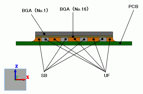
Body Attributes and Materials
|
Body Number/Type |
Body Attribute Name |
Material Name |
|
0/Sheet |
PCB |
GLASS_EPOXY |
|
1/Sheet |
BGA |
EPOXY |
|
3/Sheet |
SB |
SOLDER |
|
4/Sheet |
SB |
SOLDER |
|
5/Sheet |
SB |
SOLDER |
|
6/Sheet |
SB |
SOLDER |
|
11/Sheet |
UF |
UNDER_FILL |
|
12/Sheet |
UF |
UNDER_FILL |
|
13/Sheet |
UF |
UNDER_FILL |
|
14/Sheet |
UF |
UNDER_FILL |
|
15/Sheet |
UF |
UNDER_FILL |
|
16/Sheet |
BGA |
GLASS_EPOXY |
The material properties are set up as follows:
|
Material Name |
Tab |
Properties |
|||||
|
GLASS_EPOXY |
Elasticity |
Young’s modulus: 28×10^9[Pa] Poisson’s ratio: 0.3 |
|||||
|
Coefficient of Expansion |
Anisotropy: Select Anisotropic. Vector of expansion coefficient
|
||||||
|
EPOXY |
Elasticity |
Young’s modulus: 19×10^9[Pa] Poisson’s ratio: 0.3 |
|||||
|
Coefficient of Expansion |
11×10^-6[1/deg] |
||||||
|
SOLDER |
Elasticity |
Young’s modulus: 31×10^9[Pa] Poisson’s ratio: 0.4 |
|||||
|
Coefficient of Expansion |
21×10^-6[1/deg] |
||||||
|
UNDER_FILL |
Elasticity |
Young’s modulus: 3.5×10^9[Pa] Poisson’s ratio: 0.3 |
|||||
|
Coefficient of Expansion |
90×10^-6[1/deg] |
UF is set up as follows.
|
Body Attribute Name |
Tab |
Settings |
|
UF |
Analysis Domain |
Birth/Death Setting: Step 1: No |
Boundary Conditions
N/A
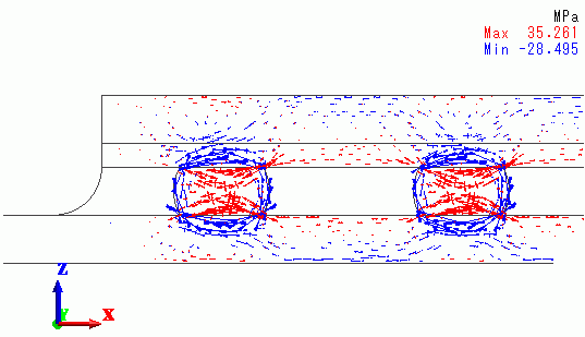
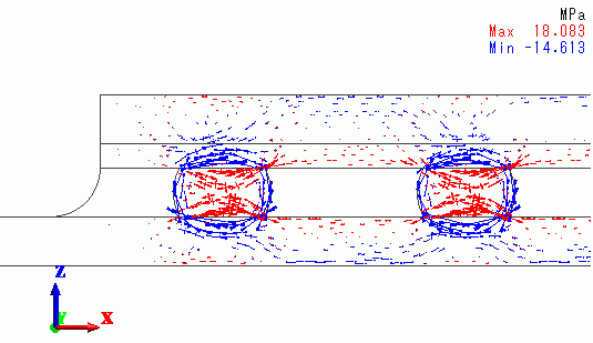
Results
The vectors of the mechanical stress at each step are shown below.
The minimum/maximum values of the vectors are set to 0 -> 200M on the vector tab of Graphics Setup.
Step 1: Reached temperature 25 [deg]:
Step 2: Reached temperature 120 [deg]:
Step 3: Reached temperature 25 [deg]:
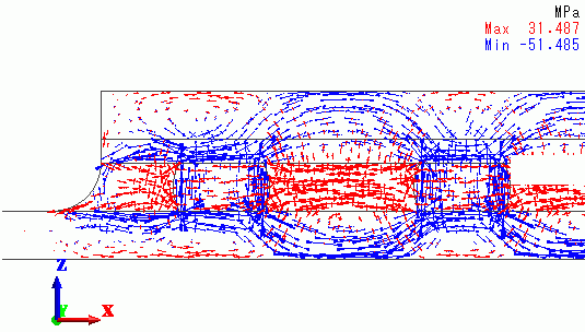
Step 4: Reached temperature 85 [deg]:
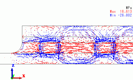
The mechanical stresses increase when the ambient temperature changes further away from the hardening temperature. .
By comparing Step 1 and Step 3, you can see that the shrinkage of the underfill causes the stress on IC and the substrate.