
CAE Software【Femtet】Murata Software Co., Ltd.
Example38 Elasto-Plastic Material Subjected to Repetitive Thermal Loading
General
-
This is an example of multi-step thermal load analysis.
-
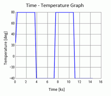
In this exercise, the solder as a temperature-dependent elasto-plastic material is subjected to the temperature cycles.
-
The plastic strains accumulate over time.
-
Unless specified in the list below, the default conditions will be applied.
Analysis Space
|
Item |
Settings |
|
Analysis Space |
Axisymmetric |
|
Model unit |
mm |
Analysis Conditions
To simplify the analysis, the axisymmetric model is analyzed.
Select the thermal load option.
|
Item |
Settings |
|
Solver |
Mechanical Stress Analysis [Galileo] |
|
Analysis Type |
Static analysis |
|
Options |
Select Thermal load. |
The Step/Thermal Load tab is set as follows.
|
Tab |
Setting Item |
Settings |
|||||||||||||||||||||||||||||||||||
|
Step/Thermal Load |
Step Setting |
Multi-step thermal load analysis |
|||||||||||||||||||||||||||||||||||
|
Time Setting |
Set up |
||||||||||||||||||||||||||||||||||||
|
Reference temperature |
25[deg] |
||||||||||||||||||||||||||||||||||||
|
Step/Reached Temperature Setting |
|
||||||||||||||||||||||||||||||||||||
|
Options for the Multi-Step Analysis |
Save the results of substeps : Select |
The reference temperature (non-stress temperature) is 25[deg]
Select [Multi-step thermal analysis] for the Step Setting, [Set up] for the Time Setting.
Also, set up in the [Step/Reached Temperature Setting].
The duration of the temperature-rise/fall steps is 300[s] = 5[min] each and the number of substeps is 10.
The duration of the temperature-keep steps is 3300[s] = 55[min] and the number of substeps is 1.
The time setting is the same as that of Exercise 39 for easy comparison.
The absolute time has no meaning when analyzing elasto-plastic materials.
The number of substeps is minimized to 1 during the temperature-keep steps as there is no change expected.
The absolute time is a physical parameter required for the creep materials analysis. Please refer to Ex-39.
By selecting “Save results of substeps”, the results at substeps can be output.
Model
A silicon chip is to be soldered on a glass-epoxy PCB.
The mesh size of the solder ball is set to 0.2.
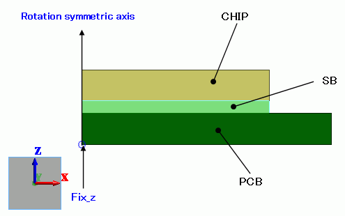
Body Attributes and Materials
|
Body Number/Type |
Body Attribute Name |
Material Name |
|
0/Sheet |
PCB |
006_Glass_epoxy |
|
1/Sheet |
SB |
SOLDER |
|
2/Sheet |
CHIP |
301_Silicon(single-crystal) |
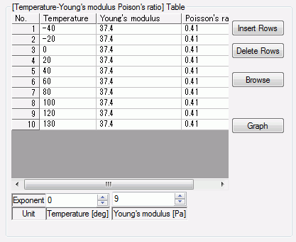
The material properties of SOLDER are set up as follows:
|
Material Name |
Tab |
Properties |
|
SOLDER |
Elasticity |
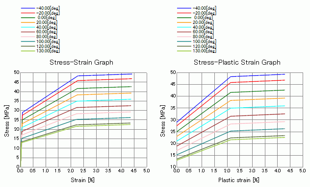
Material Type: Elasto-plastic/Multilinear Hardening Law: Kinematic hardening Temperature Dependency Yes Material Property:
[Temperature-Young’s modulus Poison’s ratio] Table:
[Plastic strain-Stress] Multilinear: omitted due to too many points See the graphs below.
Stress-Strain Graph, Stress-Plastic strain Graph
|
|
Coefficient of Expansion |
23×10^-6[1/deg] |
Boundary Conditions
|
Boundary Condition Name/Topology |
Tab |
Boundary Condition Type |
Settings |
|
Fix_z/Vertex |
Mechanical |
Displacement |
Select the Z-direction component. UZ=0 |
Results
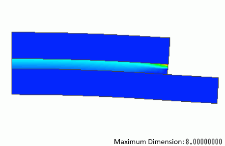
The accumulated equivalent plastic strain at time 14400[s] is shown below.
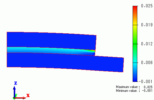
High strains are exhibited at the border of SB and CHIP.
Strains are concentrated at the top right corner of the solder.
The accumulated equivalent plastic strain over time is shown below.
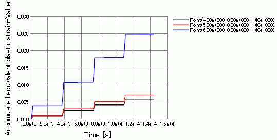
The plastic strains accumulate over time.
There is no change while the temperature remains the same.
The von Mises equivalent stress at the border of SB and CHIP over time is shown below.
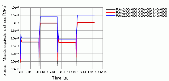
The stress is higher at the low-temperature period than at the high-temperature period.
This is because the temperature difference from the reference is larger and the solder’s yield stress is higher at low temperature.