


|
Home / Examples / Electric Analysis [Coulomb] / Example 10: Hall Element Analysis
Example 10: Hall Element Analysis
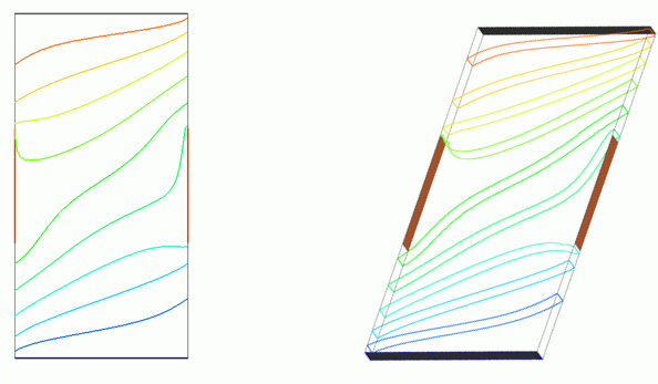
General
-
The magnetic field is applied vertically to the p-type or n-type semiconductor and runs the current.
The charged particles flowing through the sample are subjected to Lorentz force by the magnetic field and move perpendicular to the current and magnetic field.
This results in the electric field perpendicular to both the current and the magnetic field. This phenomenon is known as the Hall effect.
-
The Hall voltage and the resistance in response to the applied magnetic field with the Hall effect taken into account are solved in this example.
-
A 2D model and a 3D model are analyzed to see the thickness effect of the hall element in this example.
-
Unless specified in the list below, the default conditions will be applied.
-
Obtain this session's project file. (Right-click and choose 'Save link as')
-
Results will vary depending on Femtet version and the PC environment.
Analysis Space
|
Item |
Settings |
|
Analysis Space |
2D and 3D |
|
Model unit |
mm |
Analysis Conditions
|
Item |
Settings |
|
Solver |
Electric Analysis [Coulomb] |
|
Analysis Type |
Static Analysis (Resistance) |
|
Options |
Select [Perform the Hall element analysis]. |
Define the external magnetic field.
In a 3D model, magnetism is applied in the -Z direction to align the direction of the 2D model and the Hall electric field.
|
Tab |
Setting Item |
Settings |
|
External Magnetic Field (2D) |
External magnetic field |
Y component: 79577 [A/m] |
|
External Magnetic Field (3D) |
External magnetic field |
Z component: -79577 [A/m] |
Model
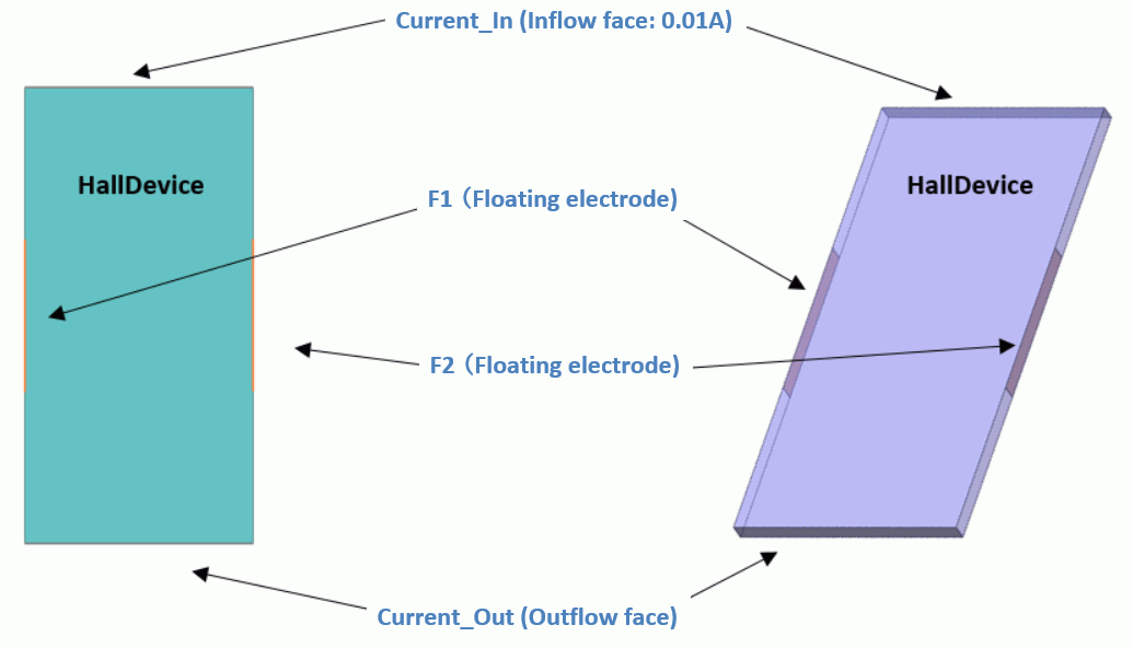
In a 2D model, a sheet body represents the Hall device. The electrodes to apply the current and floating electrodes to obtain the Hall voltage are set on the circumferential edges.
In a 3D model, a sheet body represents the Hall device. The electrodes to apply the current and floating electrodes to monitor the Hall voltage are set on the circumferential edges.
Body Attributes and Materials
|
Body Number/Type |
Body Attribute Name |
Material Name |
|
0/Sheet (2D) |
HallDevice |
HallDevice |
|
4/Solid (3D) |
HallDevice |
HallDevice |
In the 3D model, the thickness (height) of the Hall device is set at 0.01 mm to see the effect of the thickness.
|
Body Attribute Name |
Thickness/Height |
|
HallDevice (2D) |
Thickness of Sheet Body: 3×10⁻³ [mm] |
|
HallDevice (3) |
0.01 [mm] |
|
Material Name |
Conductor wall |
|
HallDevice |
Conductivity Type: Semiconductor Coefficient of Hall: 3.5×10⁻⁴ [m3/C] Hall Mobility: 7.4 [m2/V/sec] |
Boundary Conditions
Set applied current to Current_In. Current_Out is an outflow face of current. F1 and F2 are floating electrodes.
|
Boundary Condition Name/Topology |
Tab |
Boundary Condition Type |
Settings |
|
Current_Out/Edge and Face |
Electric |
Electric Wall |
Current Specified (Inflow Face) 0.01 [A] |
|
Current_In/Edge and Face |
Electric |
Electric Wall |
Current Specified (Outflow Face) |
|
F1/Edge and Face |
Electric |
Electric Wall |
Floating Electrode |
|
F2/Edge and Face |
Electric |
Electric Wall |
Floating Electrode |
Results
To view the calculation results, go to the [Results] tab

and click [Show Numerical Summary Table] .
.
In the 2D model, the floating electrodes are as follows.
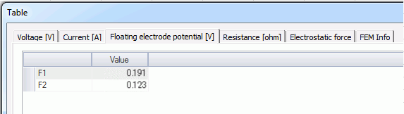
The electric potential difference between F1 and F2 is the Hall voltage.
In the 3D model, the Hall voltage is as follows. The difference from the 2D model is generated due to the effect of the thickness.
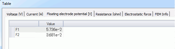
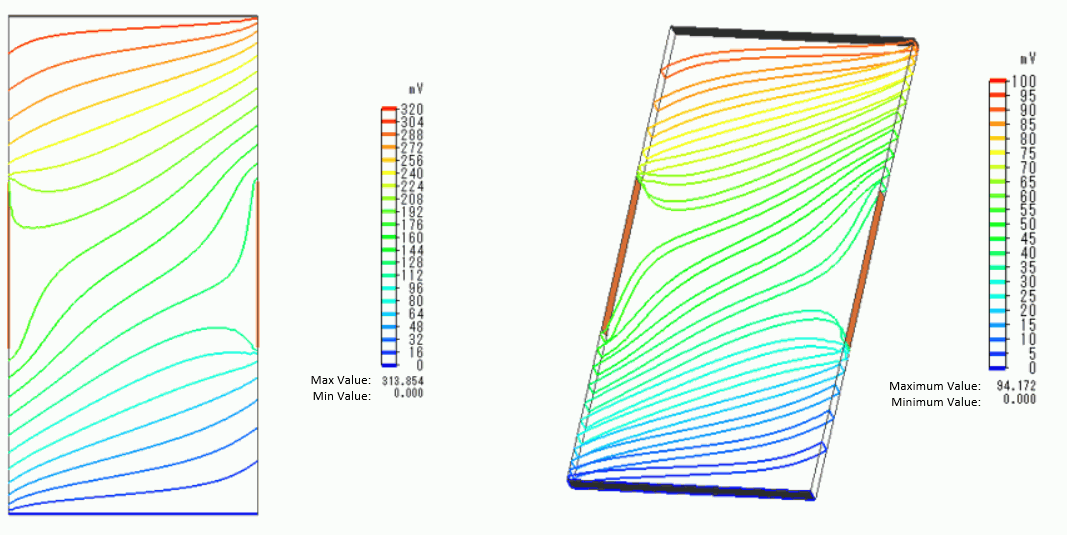
The isoline contour of the electric potential is shown below.
The number of divisions in the Color Setting is 20 on the Contour tab of Graphics Setup dialog box.
The vectors of the current density are shown below.
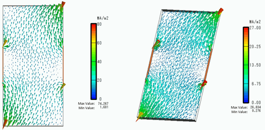
You can see that the distributions of electric potential and current are disturbed due to the Hall effect.