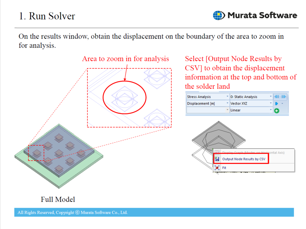

| General | When analyzing the stress on the solder bump in a stress analysis of a package on a substrate, if meshes are created according to the size of the solder bump, the calculation load may become large in some cases. In such a case a zooming analysis will allow high analysis accuracy without increasing the analysis load. |
|---|---|
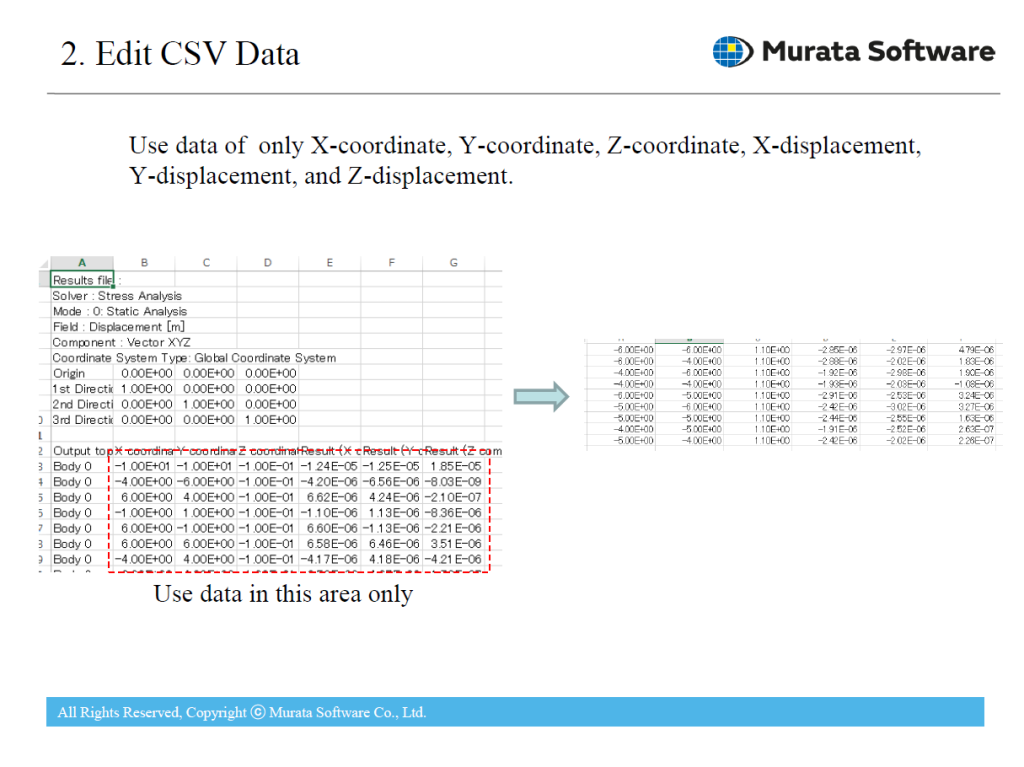
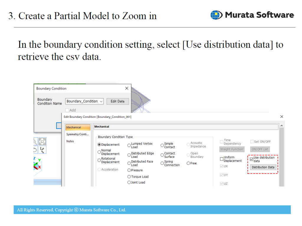
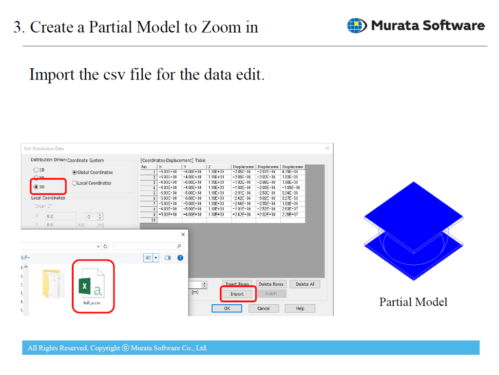
| Analysis Model | Fig. 1 shows an analysis model. The electronic components such as IC and LED are placed on the substrate. The analysis steps are; (1) Run solver. (2) Extract the node results (csv) for zooming analysis, (3) Edit the csv data. (4) Create a partial model of the area for zooming analysis. Use the distributed load as a boundary condition. |
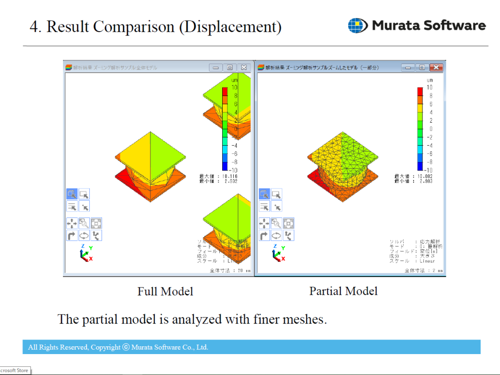
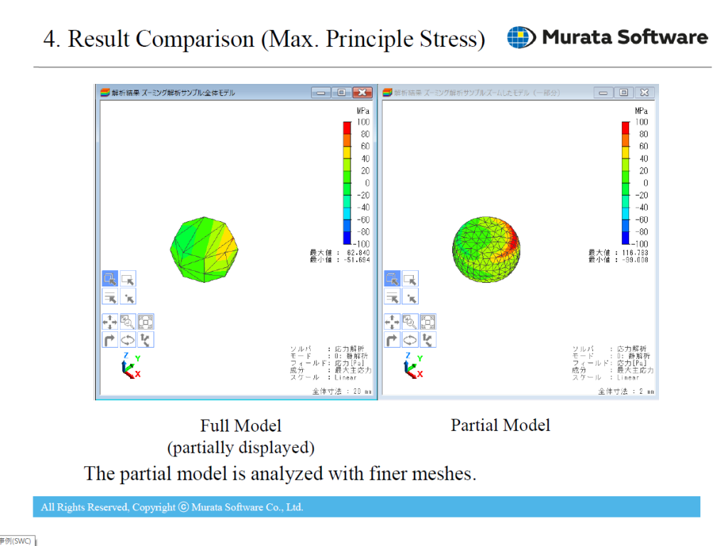
| Result | As the results show, the partial model is analyzed with the finer meshes. |
| Keywords | Zooming Analysis,Mesh,Solder Bump,Stress Analysis,Heat Conduction Analysis |