
CAE Software【Femtet】Murata Software Co., Ltd.
Example10 Hall Element Analysis
General
-
In the p-type (or n-type) semiconductor, the current flows in Z direction where the magnetic field exists in y direction.
Charged particles move in x direction due to the Lorentz force.
This results in Hall effect: the production of electric field perpendicular to both the current and the magnetic field.
-
The Hall voltage and the resistance are solved in this exercise.
-
Unless specified in the list below, the default conditions will be applied.
Analysis Space
|
Item |
Settings |
|
Analysis Space |
2D |
|
Model unit |
mm |
Analysis Conditions
The analysis space is 2D only for Hall element analysis.
|
Item |
Settings |
|
Solvers |
Electric Field Analysis [Coulomb] |
|
Analysis Type |
Static analysis |
|
Material Type |
Conductor |
|
Options |
Select “Perform the Hall element analysis”. |
Define the external magnetic field.
|
Tab |
Setting Item |
Settings |
|
External magnetic field |
External magnetic field |
Y component: 79577[A/m] |
Model
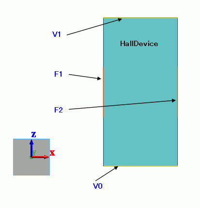
A sheet body represents the device. The electrodes to apply the voltage and to monitor the Hall voltage are set on the circumferential edges.
Body Attributes and Materials
|
Body Number/Type |
Body Attribute Name |
Material Name |
|
0/Sheet |
HallDevice |
HallDevice |
|
Body Attribute Name |
Thickness/Width |
|
HallDevice |
Thickness of Sheet Body: 3×10^-3[mm] |
|
Material Name |
Conductor wall |
|
HallDevice |
Conductivity Type: Semiconductor Hall coefficient: 3.5×10^-4[m3/C] Hall mobility: 7.4[m2/V/sec] |
Boundary Conditions
Set voltages on V0 and V1. F1 and F2 are floating.
|
Boundary Condition Name/Topology |
Tab |
Boundary Condition Type |
Settings |
|
V0/Edge |
Electric |
Electric wall |
Voltage specified, 0[V] |
|
V1/Edge |
Electric |
Electric wall |
Voltage specified, 1[V] |
|
F1/Edge |
Electric |
Electric wall |
Floating Electrode |
|
F2/Edge |
Electric |
Electric wall |
Floating Electrode |
Results
To view the calculation results, go to the [Results] tab

click [Table] ![]() .
.
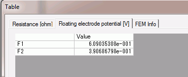
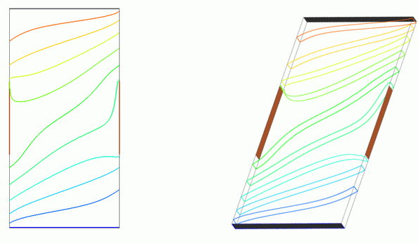
The potential difference between F1 and F2 is the Hall voltage.
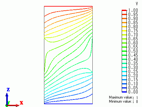
The isoline contour of the potential is shown below.
The contour’s division is set to “Equal spacing” and the division number is 20 on the Contour tab of Graphics Setup dialog box.
The vectors of the current density are shown below.
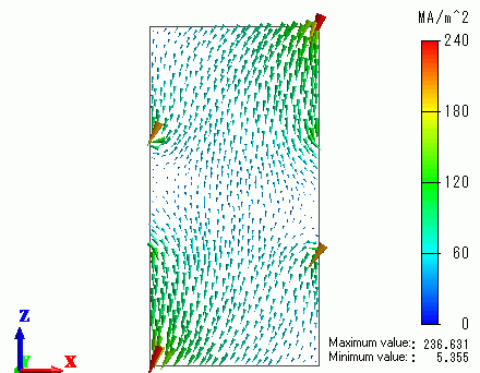
You can see that the distributions of potential and current are disturbed due to the Hall effect.