
CAE Software【Femtet】Murata Software Co., Ltd.
Example39 Charge and Discharge of Capacitor
General
-
The process of charging and discharging capacitor is analyzed. The capacitor is set as a lumped constant boundary.
-
The current discharged from the capacitor can be used as a current waveform for the ESD test.
-
Unless specified in the list below, the default conditions will be applied.
-
Electromagnetic-transient analysis is available in an optional package.
Analysis Condition
|
Item |
Setting |
|
Solver |
Electromagnetic Analysis [Hertz] |
|
Analysis Space |
3D |
|
Analysis Type |
Transient Analysis |
|
Unit |
mm |
|
Tab |
Setting Item |
Setting |
|
Mesh |
Frequency-Dependent Meshing |
|
|
Transient Analysis |
|
Finish Time of Calculation
Deselect End automatically if the ratio residual fields falls below the threshold |
Model
The process of charging and discharging capacitor depends on the circuit configuration where the capacitor is used. The discharged current of capacitor used for the ESD testing
has a transitional waveform. The circuit is configured so as to reproduce the environment where the ESD testing is conducted.
In this example, two types of circuits are prepared for the ESD testing at the component level.
-
HBM (Human Body Model) Fig. 1 left: Simulates the discharged current from a human body. Capacitor and resistor are placed in series in the RC circuit.
-
MM (Machine Model) Fig. 1 right: Simulates the discharged current from a metal device. Capacitance, inductor, and resistor are placed in series in the RLC circuit.

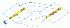
Fig. 1: Capacitor and Circuit (left: HBM, right: MM)
Body Attributes and Materials
|
Body Number/Type |
Body Attribute Name |
Material Name |
|
Body0/Solid |
SUBSTRATE |
006_Glass_epoxy * |
|
Body1/Solid |
AIR |
000_Air * |
|
Body2, Body4, Body6/Sheet (HBM) Body2, Body4, Body6, Body8/Sheet (MM) |
ELECTRODE |
003_Ag |
(*) Available from the material DB
Boundary Condition
|
Boundary Condition Name/Topology |
Tab |
Boundary Condition Type |
Setting |
||||||||||||||||||||
|
V/Face |
Electric |
Port |
Integral Path:
Voltage Port
Input Waveform (HBM)
Input Waveform (MM)
|
||||||||||||||||||||
|
C/Face |
Electric |
Lumped constant |
Capacitance
Set the integral path* |
||||||||||||||||||||
|
R/Face |
Electric |
Lumped constant |
Resistance
Set the integral path* |
||||||||||||||||||||
|
L/Face |
Electric |
Lumped constant |
Inductance
Set the integral path* |
||||||||||||||||||||
|
Ground/Face |
Electric |
Electric wall |
|
||||||||||||||||||||
|
Outer Boundary Condition |
Electric |
Open boundary |
* The integral path on the lumped constant boundary is set so as to connect the conductors that are in contact with the lumped constant boundary.
Results
The result table of the electromagnetic analysis (time domain) will display the voltage and current on the lumped constant boundary, and the current in the ports.
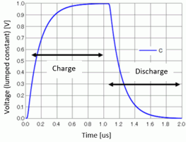
HBM
The voltage on the capacitor is as shown in Fig. 2. While the voltage is applied to the port, the capacitor is charged for up to 1.0 [ns].
At 1.0 [ns], when the port is short-circuited, the discharge begins.
The voltage Vc [V] at the time t [s] in the RC circuit is obtained theoretically as follows.
Vc = V0 × (1- exp(-t/RC))
where V0 is direct voltage connected to the circuit, R is resistance, and C is capacitance.
From this equation, the time taken to charge 99% of the capacitor (Vc=0.99V0) is about 690 [ns]. As shown in the analysis result (Fig. 2), the time taken to charge 99% of the capacitor
is 720 [ns]. This is close to the theoretical value of 690 [ns] and confirms that the analysis is correctly performed.
The difference between the theoretical value and the analysis result is due to the rise time of the voltage waveform applied to the port. If the rise time is shorter, the difference will become smaller.
However, if the rise time is shorter, the timestep for analysis will become smaller and the analysis time will become longer.

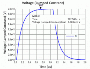
Fig. 2: Charge and Discharge of Capacitor (HBM)
The current discharge in the HBM can be confirmed by the current flowing through the port. The result is shown below.
The current flowing into the model from the port is treated as positive. Therefore the current in the discharge process (after 1.0[ns]) is negative.
As shown in Fig. 3, the pulse rises up steeply and then the current is slowly damped.

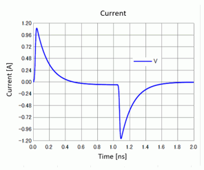
Fig. 3: Charge and Discharge Current (HBM)
MM
The voltage on the capacitor is as shown in Fig. 4. The discharge current from the capacitor is shown in Fig. 5.
The behaviors of voltage and current in the RLC circuit largely depend on the values of R, L, and C. In a circuit like MM having small resistance value,
the discharge current which is oscillated by C and L shows damped oscillation where the amplitude of oscillation gradually reduces due to R.
Actually, as shown in Fig. 5, the discharge current from the port shows damped oscillation.

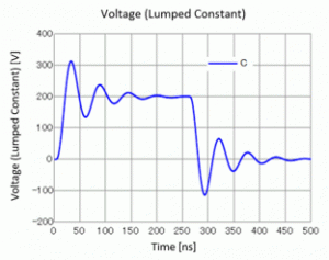
Fig. 4: Charge and Discharge of Capacitor (Voltage)

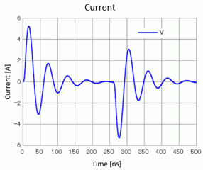
Fig. 5: Discharge Current from Capacitor