
CAE Software【Femtet】Murata Software Co., Ltd.
Example22 Measurement of the Junction Thermal Resistance
General
-
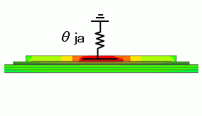
The thermal resistances θ ja, θ jc, θ jb, and the thermal parameters Ψ jt and Ψ jb of the semiconductor package are solved.
Refer to Results Obtained in the Thermal Analysis (Table)] for the thermal resistance of the semiconductor package.
-
The first Model is the natural convection environment. The junction-ambient thermal resistance θ ja and heat parameters Ψ jt and Ψ jb are obtained.
-
The second Model radiates the heat through the package surface only. The junction-package thermal resistance θ jc is obtained.
-
The third Model radiates the heat through the substrate surface only. The junction-substrate thermal resistance θ jb is obtained.
-
Unless specified in the list below, the default conditions will be applied.
Analysis Conditions
|
Item |
Setting |
|
Solver |
Thermal Analysis [Watt] |
|
Analysis Space |
3D |
|
Analysis Type |
Steady-state analysis |
|
Model unit |
mm |
|
Options |
N/A |
Graphical Objects
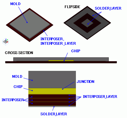
Semiconductor package model
The package is a BGA type consisting of silicon chip, junction, interposer, mold resin, and solder. The dimensions are 35mm x 35mm.
The junction is a sheet body. It is placed on the chip and the heat source is applied.
The interposer consists of four wiring layers and three insulating layers.
In actuality, the soldering is performed with several hundred of solder bumps. In this exercise, for the purpose of reducing the calculation time,
two models are created for the solder areas (peripheral and center). Equivalent anisotropic thermal conductivity is set as the material property.
The mesh size is 1.0 for silicon chip, junction, interposer, and mold resin.
The mesh of the solder is the default size of 5.0.
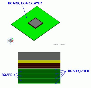
Measuring substrate model
A four-layer model (101.6mmx114.3mmx1.6mm) is created which is consisted of four wiring ayers and three insulating layers. The dimensions are.
The dimensions conform to the JEDEC standard.
The general mesh size of 5.0 is applied to the measuring substrate.
It is used for the Models 1 and 3.
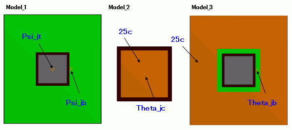
Model 1
A semiconductor package model is placed on the measuring substrate model.
Point bodies are placed where Ψjt (center of the top surface) and Ψjb (1mm off the edge of substrate) are measured, and “measuring terminal” boundary condition is applied.
The measuring environment stipulated by the JEDEC standard is natural convection in the closed container.
But in this exercise, the container is ignored. For the outer boundary condition, the “Heat Transfer/Ambient Radiation” is selected and Natural convection (automatic calculation) and Ambient radiation are selected.
Model 2
The semiconductor package model is used.
In order to reproduce the measuring environment set by JEDEC standard where a cold plate is put on the top surface of the model,
“Temperature” boundary condition is applied to the top surface.
Point body is placed where θjc (center of the top surface) is measured, and “measuring terminal” boundary condition is applied.
The outer boundary condition is default setting of “Adiabatic”.
Model 3
A semiconductor package model is placed on the measuring substrate model.
In order to reproduce the measuring environment set by JEDEC standard where a cold plate is placed between the cold plates.
The area where the cold plate contacts is created as a sheet body.
“Temperature” boundary condition is applied.
Point body is placed where θjb (1mm off the edge of substrate) is measured, and “measuring terminal” boundary condition is applied.
Body Attributes and Materials
Body attributes and materials of Model 1
|
Body Number/Type |
Body Attribute Name |
Material Name |
|
0/Solid |
CHIP |
Si |
|
1,3,5,7/Solid |
LAYER |
008_Cu *1 |
|
2,4,6/Solid |
INSULATION_LAYER |
006_Glass_epoxy *1 |
|
8/Solid |
MOLD |
MoldResin |
|
9,12/Solid |
SOLDER_LAYER |
Solder_Aniso |
|
13/Face |
JUNCTION |
Si |
|
14,16,17,18/Solid |
BOARD_LAYER |
008_Cu *1 |
|
15/Solid |
BOARD |
006_Glass_epoxy *1 |
|
19,20/Vertex |
No setup *2 |
No setup *2 |
*1 Available from the Material DB.
*2 Imprinting body for the boundary condition.
Body attributes and materials of Model 2
|
Body Number/Type |
Body Attribute Name |
Material Name |
|
0/Solid |
CHIP |
Si |
|
1,3,5,7/Solid |
LAYER |
008_Cu *1 |
|
2,4,6/Solid |
INSULATION_LAYER |
006_Glass_epoxy *1 |
|
8/Solid |
MOLD |
MoldResin |
|
9,12/Solid |
SOLDER_LAYER |
Solder_Aniso |
|
13/Face |
JUNCTION |
Si |
|
19/Vertex |
No setup *2 |
No setup *2 |
*1 Available from the Material DB.
*2 Imprinting body for the boundary condition.
Body attributes and materials of Model 3
|
Body Number/Type |
Body Attribute Name |
Material Name |
|
0/Solid |
CHIP |
Si |
|
1,3,5,7/Solid |
LAYER |
008_Cu *1 |
|
2,4,6/Solid |
INSULATION_LAYER |
006_Glass_epoxy *1 |
|
8/Solid |
MOLD |
MoldResin |
|
9,12/Solid |
SOLDER_LAYER |
Solder_Aniso |
|
13/Face |
JUNCTION |
Si |
|
14,16,17,18/Solid |
BOARD_LAYER |
008_Cu *1 |
|
15/Solid |
BOARD |
006_Glass_epoxy *1 |
|
21,22/Face |
No setup *2 |
No setup *2 |
|
23/Face |
No setup *2 |
No setup *2 |
*1 Available from the Material DB.
*2 Imprinting body for the boundary condition.
Heat source and thickness are given to JUNCTION body (for Models 1, 2, and 3).
|
Body Attribute Name |
Tab |
Setting |
|
JUNCTION |
Heat Source |
2[W] |
|
Thickness/Width |
Thickness of sheet body: |
If the material DB is not used, the material property below is applied (for Models 1, 2, and 3).
|
Material Name |
Tab |
Setting |
|||||||||
|
Si |
Thermal Conductivity |
120[W/m/deg] |
|||||||||
|
Mold_Resin |
Thermal Conductivity |
0.8[W/m/deg] |
|||||||||
|
Solder_Aniso |
Thermal Conductivity |
Anisotropy: Select “Anisotropic”. Set up Anisotropic Thermal Conductivity *1
|
Note *1) The set up is as follows.
As the thermal conductivity in the 1st and 2nd directions (plane) is blocked by air, the value of [000_Air] in the material DB is set to 0.0293[W/m/deg].
For the 3rd direction (height), the value for [107_Lead-free_solder_SnAgCu] of the material DB is defined by the area of solder layer model and
the actual ratio of solder bump area to the layer area.
Assuming the actual terminal pitch of the solder bump is 1[mm] and diameter of bump is 0.35[mm],
the ratio of bump area / rectangle area surrounding a bump = π x 0.35 x 0.35 /( 1 x 1 ) = 0.384845
Thermal conductivity of the 3rd direction = 64 x 0.384845 = 24.81 [W/m/deg]
Boundary Conditions
For Model 1, measuring terminal boundary condition is set, and natural convection and ambient radiation are selected for the outer boundary condition.
For Model 2, temperature boundary condition is set. Unlike Model 1, the outer boundary condition is “Adiabatic”.
For Model 3, temperature boundary condition and measuring terminal boundary condition are set. Unlike Model 1, the outer boundary condition is “Adiabatic”.
|
Boundary Condition Name/Topology |
Tab |
Boundary Condition Type |
Setting |
|
Psi_jt/Vertex (Model 1) |
Thermal |
Measuring Terminal |
N/A |
|
Psi_jb/Vertex (Model 1) |
Thermal |
Measuring Terminal |
N/A |
|
Outer Boundary Condition (Model 2, Model 1) |
Thermal |
Heat Transfer/Ambient Radiation |
Room temperature (ambient temperature): 25[deg] Radiation rate: 0.8 |
|
25c/Face (Model 2, Model 3) |
Thermal |
Temperature |
25[deg] |
|
Outer Boundary Condition (Model 2, Model 3) |
Thermal |
Adiabatic |
N/A |
|
Theta_jc/Vertex (Model 2) |
Thermal |
Measuring Terminal |
N/A |
|
Theta_jb/Vertex (Model 3) |
Thermal |
Measuring Terminal |
N/A |
Results
The results in [Junction Thermal Resistance] of the output table for Model 1 are shown as below.
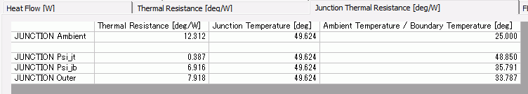
As in the table, you can see the followings.
Junction – Ambient Thermal Resistance θa = 12.312 [deg/W]
Heat Parameter Ψjt = 0.387 [deg/W]
Heat parameter Ψjb = 6.916 [deg/W]
The results in [Junction Thermal Resistance] of the output table for Model 2 are shown as below.
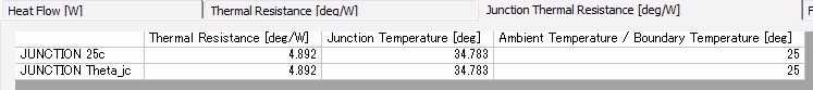
As in the table, you can see the following.
Junction-Package Surface Thermal Resistance θjc = 4.892 [deg/W]
The results in [Junction Thermal Resistance] of the output table for Model 3 are shown as below.
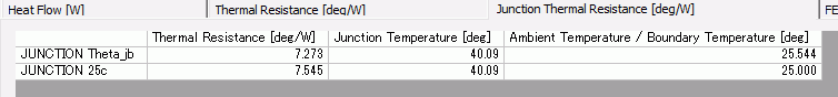
As in the table, you can see the following.
Junction-Substrate Thermal Resistance θjb = 7.258 [deg/W]