CAE Software【Femtet】Murata Software Co., Ltd.
Example9 Plating Analysis(Plating a Device in the Bath)
General
-
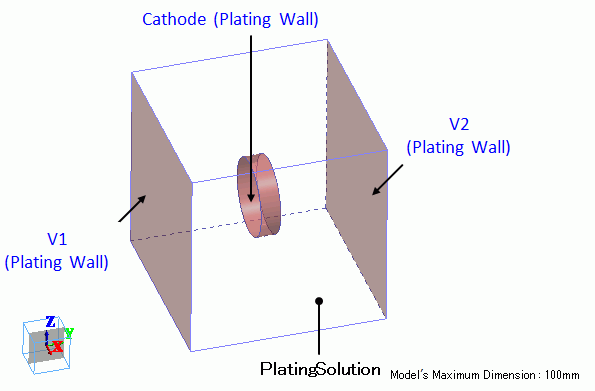
Simulation model is created which will be immersed in the plating bath and plated.
-
By modeling the anode and cathode, distribution of electric potential at the electrodes can be taken into account.
-
Explanation of how to create the model using plating wall will be given at the end of this Exercise.
-
Unless specified in the list below, the default conditions will be applied.
Analysis Space
|
Item |
Setting |
|
Analysis Space |
3D |
|
Model unit |
mm |
Analysis Conditions
The material is conductor for the plating analysis.
Select the [Perform the plating analysis] option.
|
Item |
Setting |
|
Solver |
Electric Field Analysis [Coulomb] |
|
Analysis Type |
Static analysis |
|
Material |
Conductor |
|
Options |
Select Perform the plating analysis |
|
Meshing Setup |
General mesh size: 6.0 [mm]*1
Meshing Control |
|
Matrix Solver Type |
Direct method*3 |
-
*1: Mesh size of 6.0mm is set as the simulation accuracy will not be enough with the automatically-set mesh size of 12.0mm.
-
*2: By this setting, the curved face can be meshed more smoothly.
See [Meshing Control] for the detail.
-
*3: In the electric field analysis, if Automatic is selected for the Matrix Solver Type, the iterative method is used.
In this Exercise, Direct Method is selected as it converges faster than Iterative Method.
Graphical Objects
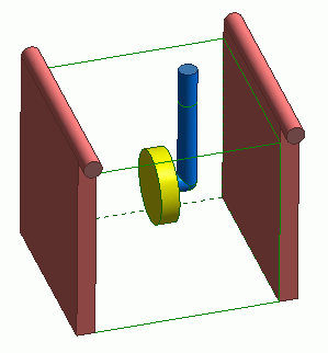
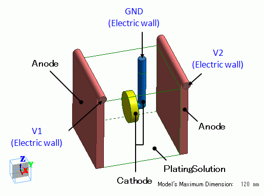
Box body (green) is the plating solution. As the target object for plating, a disc part (yellow) is placed in the box.
The disc part is a cathode. Anodes (red) are placed on both sides of the disc part.
Assuming that the protruding portion of the cylinder on top of the anodes are connected to the current power source, electric walls V1 and V2 are set on the anodes.
The conductor (blue) is connected to the disc part. It is for supporting the disc part as well as for the current flow.
The electric wall GND is set on the tip of the conductor assuming it is connected to the ground.
Body Attributes and Materials
Create solid bodies for the plating bath, the anodes, the disc part (cathode), and supporter of the disc part (conductor). Body attributes are plating solution and metal.
|
Body Number/Type |
Body Attribute Name |
Material Name |
|
3/Solid |
Cathode |
Metal |
|
9/Solid |
Anode |
Metal |
|
10/Solid |
Anode |
Metal |
|
11/Solid |
Cathode |
Metal |
|
12/Solid |
Plating Solution |
Solution |
The body attribute is set as follows.
|
Body Attribute Name |
Plating Tab |
||||||||||||||
|
Anode |
Type of Plating Body: Anode
Overvoltage Type: Linear
|
||||||||||||||
|
Cathode |
Type of Plating Body: Cathode
Overvoltage Type: Tafel’s Law
|
||||||||||||||
|
Plating Solution |
Type of Plating Body: Plating Solution
|
||||||||||||||
The material properties are set as follows.
|
Material Name |
Conductivity Tab |
|
Metal |
Conductivity Type: Conductor Conductivity: 10×106 [S/m]
|
|
Solution |
Conductivity Type: Conductor Conductivity: 10 [S/m]
|
Boundary Condition
The boundary conditions are set as follows.
|
Boundary Condition Name/Topology |
Tab |
Boundary Condition Type |
Setting |
|
Ground/Face |
Electric |
Electric wall |
Ground |
|
V1/Face |
Electric |
Electric wall |
Current 1A |
|
V2/Face |
Electric |
Electric wall |
Current 1A |
Results
Current density of the plating solution is shown in the Figure 1.
All bodies except plating solution body are not shown because
current density of the plating solution cannot be seen due to the current density of electrodes if the electrode bodies are shown.
The current from the anodes is observed to flow to the cathode which consists of the disc part and the supporting body.
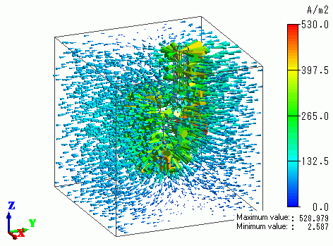
Figure 1 The distribution of the current density in the plating solution
-
Between the bodies with attributes of electrodes (anode and cathode) and the plating solution,
a body with body attribute name of RESERVED_dual is automatically created.
The vector field (electric field or current density) of this body is invalid.
Hide the body with attribute name of RESERVED_dual before confirming the field.
Please enter.
In the Figure 2, the current density (normal component) of the disc part’s surface is shown. In the Figure 3, the extracted plating thickness of the disc part is shown.
Both are shown in the contour and only disc part body is shown.
The Figures below, you are seeing the side having a supporting body.
The supporting body is placed upward from the center.
In the Figure 2, you can see the current density at the upper area of the part is small due to the blocked current by the supporting body.
Figure 3 shows that the plating thickness is distributed according to the current density distribution.
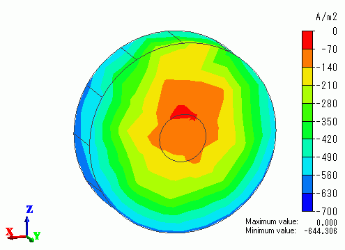
Figure 2 Current density (normal component) of the surface of the disc part
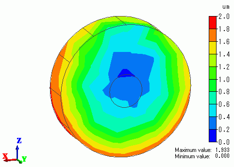
Figure 3 The extracted plating thickness of the disc part
The contour of the voltage of one of the anodes is shown in the Figure 4.
You can see that there is voltage distribution in the anode and the distribution is taken into account in the analysis.
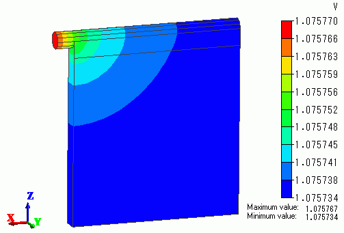
Figure 4 The voltage distribution of the anode
Model with plating wall
In this exercise, the bodies are created for anode and cathode.
The merit of doing so is voltage distribution in the electrodes can be taken into account.
It, however, increases the number of meshes according to the number of electrodes and takes longer time to simulate.
If the plating wall instead of the electrode is used for the boundary condition, though the voltage distribution in the electrode cannot be taken into account,
the calculation time is expected to be shorter because the electrode meshing is not required.
Figure 5 shows the model with the plating wall replacing the electric wall.
The plating solution body is cut out and hollow at where the disc part is supposed to be.